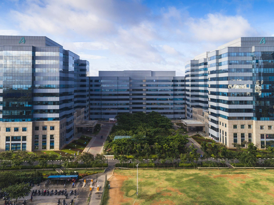
Applied Materials has announced the expansion of its Bengaluru operations with a new 8.06 lakh sq. ft. workplace at the International Tech Park. This state-of-the-art facility is set to enhance the company’s R&D, product engineering, validation, and simulation capabilities in India.
Facility Highlights
- The Bengaluru site complements the India validation center, which is the only site in the country capable of processing 300mm wafers.
- It incorporates sustainability-focused designs, including daylight-led lighting, energy-efficient systems, and responsible materials.
- Inclusive workspaces feature curated Indian art installations, reflecting local culture and employee engagement.
Supporting AI and Semiconductor Innovation
The facility works alongside Applied Materials’ AI Centre of Excellence in Chennai, driving manufacturing automation and semiconductor equipment design.
This expansion underscores India’s growing role in global semiconductor GCC operations, enabling enterprise-grade innovation and scalability.
Leadership Perspective
Priyank Kharge, Karnataka Minister for Electronics, IT & BT: Karnataka continues to be a hub for semiconductor design and manufacturing.
Avi Avula, President, Applied Materials India: “This investment comes at a pivotal moment for India’s rapidly advancing semiconductor ecosystem.”
Enterprise Impact
The expansion strengthens Applied Materials’ ability to deliver end-to-end engineering and validation services from India, positioning Bengaluru as a key global capability center hub for the company. It reflects confidence in the region’s talent, infrastructure, and strategic importance in the global semiconductor landscape.
Visit Our News section and follow us on LinkedIn and Twitter
Read more full news: Here